
 By Adri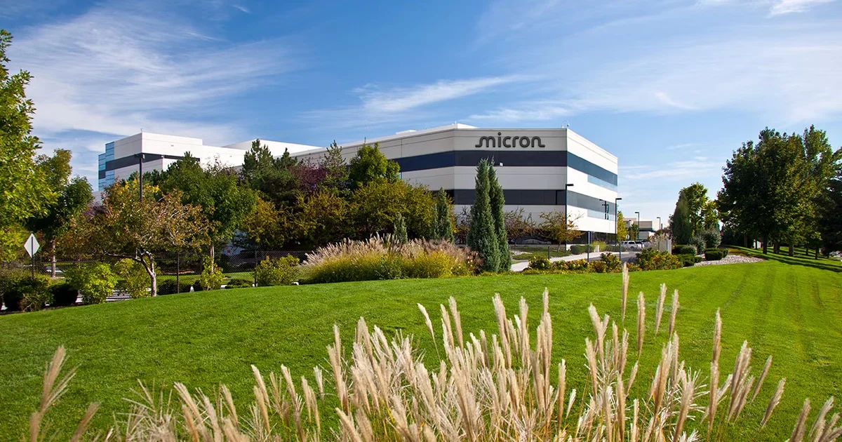
$10 billion over ten years
Micron officially unveiled Micron Research Labs on August 20, 2026. The organization will be headquartered in Boise, Idaho, where the company already operates major research activities and is expanding its manufacturing footprint.
The planned investment totals $10 billion over the coming decade.
That money is not simply the construction budget for one building. Micron also plans to fund university collaborations, global satellite laboratories and partnerships throughout the semiconductor ecosystem.
Construction of the flagship Boise facility is expected to begin in 2027, with space for hundreds of researchers.
This is not a new $10 billion memory fab
That distinction matters because Micron already has a massive US manufacturing investment program underway.
Micron Research Labs is primarily a research institution. The company wants it to explore technologies beyond its current product roadmaps and explicitly describes research extending beyond a ten-year horizon.
The new Boise DRAM fab is a separate project. Construction began years earlier, with Micron expecting meaningful DRAM output from the site in 2027.
The lab and the fab can naturally support one another, but describing the announcement simply as Micron building a $10 billion memory factory would be inaccurate.
The research goes beyond making HBM faster
Micron lists foundational memory technologies, advanced memory and compute architectures, packaging and future semiconductor manufacturing among the new lab's main research areas.
That wording matters because it suggests the company is not merely trying to increase the capacity or bandwidth of existing memory designs.
As accelerators become faster, the way data moves between memory and compute units becomes an architectural problem of its own.
A chip capable of performing enormous numbers of operations can only deliver that performance if data reaches it quickly enough and within acceptable power limits.
Memory is no longer a secondary GPU component
The rise of HBM illustrates that transformation particularly well.
Modern AI accelerators place multiple stacks of very high bandwidth memory close to the processor through advanced packaging technologies.
Memory therefore becomes a fundamental part of accelerator design. Capacity influences how much of a model or dataset can remain close to the compute units, while bandwidth affects how much work those units can actually sustain.
Adding more arithmetic performance without solving the memory problem can simply create a more expensive GPU that waits faster.
Packaging is becoming almost as strategic as the chips
Micron also lists advanced packaging as one of the laboratory's major areas of research.
The reason is straightforward. Modern AI systems increasingly need to bring different components together: accelerators, HBM stacks, interconnects and sometimes multiple compute dies inside one package.
The challenge is therefore no longer limited to manufacturing a better memory chip in isolation.
Engineers also need to assemble more components, maintain extremely fast connections between them, remove their heat and achieve manufacturing yields that remain economically viable.
AI has changed the economics of memory
The research push comes as AI demand is already reshaping the memory market.
HBM, server DRAM and data-center storage have become critical components of new compute infrastructure.
Micron has directly linked its recent record financial performance to the strategic importance of memory in the AI era and is simultaneously increasing investment in technology, products and manufacturing capacity.
Samsung and SK Hynix are seeing the same shift. Memory manufacturers now sit at the center of a race that was previously described mainly through Nvidia, AMD and specialized accelerator designers.
Micron wants to work beyond today's roadmaps
The laboratory's long-horizon mission may be its most important characteristic.
Product teams normally work on generations whose cost targets, performance goals and launch windows are already relatively well defined.
Micron Research Labs is supposed to look further ahead, including ideas that may not become manufacturable products until the following decade.
The company also intends to connect this work more closely with universities, startups, customers and government researchers.
The aim is to explore breakthroughs that would be too uncertain or too far away to fit comfortably into a normal product-development schedule.
Boise becomes both a research center and an industrial proving ground
The choice of Boise is unsurprising.
Micron's historical headquarters and a major R&D center are already located there. The company's new leading-edge DRAM fab is also being built alongside its research activities.
That proximity can shorten the path between an idea demonstrated in research and a process that can actually be manufactured.
This is one of the semiconductor industry's recurring challenges. Showing that a technology works in a handful of samples is one thing; producing millions of units with economically viable yields is something else entirely.
Future GPUs cannot simply keep adding more compute
The current AI race can make it seem as though every new accelerator generation can solve the problem by adding more transistors and raw compute.
But the constraints are increasingly appearing elsewhere: power delivery, cooling, networking, packaging and memory.
Micron Research Labs exists in part because memory risks becoming one of those structural limits.
Future systems may need to rethink the relationship between storing data and processing it rather than simply surrounding a larger GPU with more HBM.
That is ultimately what this $10 billion investment represents. Micron is not merely betting on a temporary memory shortage caused by the AI boom. It is betting that memory architecture itself will become one of computing's central battlegrounds over the next decade.